AIP Features Professors' Research on Tuning Materials and Devices
Materials with large dielectric constants — aka "high-K materials" — have recently garnered attention for their potential use within future generations of reduced-dimension semiconductor devices.
Barium strontium titanate, one such material, possesses an inherently large dielectric constant that can be altered significantly by an applied electrical field—by as much as a factor of 10. While this property has been known to exist for more than half a century and many researchers have attempted to exploit it, the technology has been limited by the low quality of the material. By semiconductor industry standards, the material is considered to be defective.
But researchers at University of California, Santa Barbara, who began exploring thin-film tunable dielectrics using sputtered material nearly two decades ago, are now trying to leverage advanced and scalable materials deposition techniques like molecular beam epitaxy (MBE) to create tunable, high-frequency integrated circuits and devices with high-quality materials that are comparable to modern semiconductor technology.
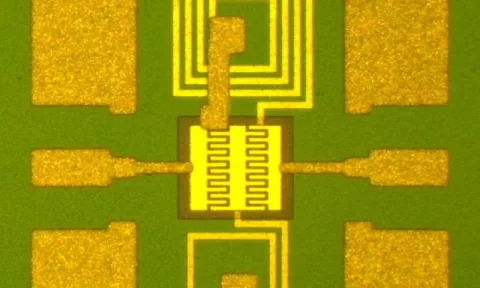
As the group reports this week in Applied Physics Letters, by using extremely high-quality epitaxial materials they were able to greatly reduce the dielectric loss in ferroelectric tunable radio-frequency (RF) capacitors. Advances at the fundamental level, such as this one, open the door to future RF materials and devices that can be electrically reconfigured or "tuned" to adapt to changing environments.
The catch is that the deposition of complex oxides, such as barium strontium titanate, is problematic because of the high temperatures and oxygen-rich environment involved.
"Our work was made possible by recent advances in a hybrid form of MBE at UCSB that uses metal organic precursors," explained Susanne Stemmer, a professor at the Materials Research Laboratory at UCSB.
The material's large dielectric constants "present fabrication challenges because the inherently high capacitance density of the films requires smaller electrode dimensions and finer lithography than many typical integrated capacitor structures," said Robert York, a professor in the Electrical & Computer Engineering department at UCSB. "Low-loss reactive devices also pose significant measurement challenges at microwave frequencies. The close collaboration of materials scientists and electrical engineers, and years of experience in device processing, was integral to the success of our work."
View the original article here.
By Staff Writer, Phys.org
This information was provided by American Institute of Physics. The American Institute of Physics (AIP) promotes science, the profession of physics, publishes physics journals, and produces publications for scientific and engineering societies.
 Facebook
 Instagram
 LinkedIn
 Twitter